ADM1073
Data Sheet
Rev. B | Page 18 of 24
FUNCTIONALITY AND TIMING
LIVE INSERTION
The timing waveforms associated with the live insertion of a
plug-in board using the ADM1073 are shown in Figure 36. The
long connector pins are the first to make connection, and the
GND V
EE
potential climbs to 48 V. As this voltage is applied,
the voltage at the V
IN
pin ramps to a constant 12.3 V and is held
at this level with the shunt resistor and external resistor
combination at the V
IN
pin. In this case, the connection pins are
staggered so that the R1/R2 and R3/R4 resistor dividers are the
last to connect to the backplane. This means that VUV and VOV
begin to ramp after the other pins connect. Note that staggered
connector pins are optional, because an internal time filter is
included on the UV pin.
When V
UV
crosses the undervoltage rising threshold, it is now
inside the operating voltage window and the 48 V supply must
be applied to the load. The SPLYGD
output is asserted and after
a time delay, tPOR, the ADM1073 begins to ramp up the gate
drive. When the voltage on the SENSE pin reaches 100 mV (the
analog current limit level), the gate drive is held constant. When
the board capacitance is fully charged, the sense voltage begins
to drop below the analog current limit voltage and the gate
voltage is free to ramp up further. The gate voltage eventually
climbs to its maximum value of 12.3 V and the
PWRGD
output
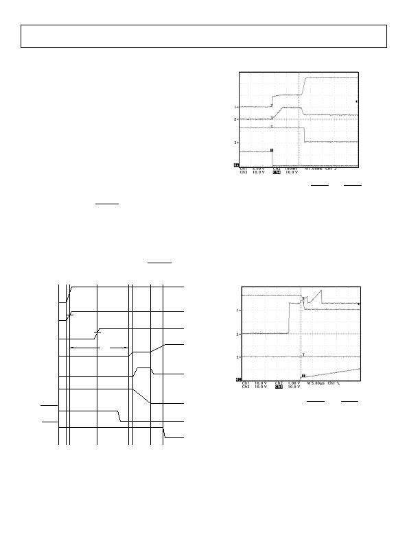
is asserted. Figure 37 shows some typical startup waveforms.
t
POR
V
LKO
V
UVR
48V RTN VEE
V
IN
V
UV
GATE
SENSE
V
OUT
SPLYGD
PWRGD
Figure 36. Timing Waveforms Associated with a Live Insertion Event
Figure 37. Typical Startup Sequence
(Ch1 = GATE; Ch2 = SENSE; Ch3 =
PWRGD
; Ch4 =
SPLYGD
)
OVERVOLTAGE AND UNDERVOLTAGE FAULTS
The waveforms for an overvoltage glitch are shown in Figure 38.
When V
OV
glitches above the overvoltage threshold of 1.93 V, an
overvoltage condition is detected and the GATE voltage is
pulled low. V
OV
begins to drop back toward the operating
voltage window, and the GATE drive is restored when the
overvoltage falling threshold (1.93 V minus preset OV
hysteresis level) is reached. Figure 38 illustrates the ADM1073s
reactions to an overvoltage condition.
Figure 38. Timing Waveforms Associated with an Overvoltage Fault
(Ch1 = GATE; Ch2 = OV; Ch3 = PWRGD
; Ch 4 = SPLYGD
)
发布紧急采购,3分钟左右您将得到回复。
相关PDF资料
ADM4210-2AUJZ-RL7
IC CTLR HOTSWAP LV TSOT23-6
ADVFC32SH
IC CONV V/F F/V MONO TO100-10
FAN4800ASNY
IC CTLR COMBO PFC/PWM 16-DIP
FAN4800AUN
IC PWM/PFC CTLR COMBO 16-MDIP
FAN4800CUN
IC PWM/PFC CTLR COMBO 16-MDIP
FAN4802MY
IC PFC CTRLR AVERAGE CURR 16SOP
FAN4802SNY
IC CTLR PFC/PWM COMBO 16-PDIP
FAN6920MRMY
IC PWM CTLR PFC/QUASI-RES 16SOP
相关代理商/技术参数
ADM1073ARU-REEL7
制造商:Analog Devices 功能描述:Hot Swap Controller 1-CH -80V 14-Pin TSSOP T/R 制造商:Analog Devices 功能描述:FULL FEATURED -48V HOT SWAP CTRL'R I.C. - Tape and Reel
ADM1073ARUZ
功能描述:IC HOTSWAP CTRLR -48V 14-TSSOP RoHS:是 类别:集成电路 (IC) >> PMIC - 热交换 系列:- 标准包装:50 系列:- 类型:热交换控制器 应用:-48V 远程电力系统,AdvancedTCA ? 系统,高可用性 内部开关:无 电流限制:可调 电源电压:11.5 V ~ 14.5 V 工作温度:-40°C ~ 85°C 安装类型:表面贴装 封装/外壳:10-TFSOP,10-MSOP(0.118",3.00mm 宽) 供应商设备封装:10-MSOP 包装:管件
ADM1073ARUZ-REEL
功能描述:IC CTRLR HOTSWAP -48V 14TSSOP RoHS:是 类别:集成电路 (IC) >> PMIC - 热交换 系列:- 标准包装:50 系列:- 类型:热交换控制器 应用:-48V 远程电力系统,AdvancedTCA ? 系统,高可用性 内部开关:无 电流限制:可调 电源电压:11.5 V ~ 14.5 V 工作温度:-40°C ~ 85°C 安装类型:表面贴装 封装/外壳:10-TFSOP,10-MSOP(0.118",3.00mm 宽) 供应商设备封装:10-MSOP 包装:管件
ADM1073ARUZ-REEL7
功能描述:IC CTRLR HOTSWAP -48V 14TSSOP RoHS:是 类别:集成电路 (IC) >> PMIC - 热交换 系列:- 标准包装:50 系列:- 类型:热交换控制器 应用:-48V 远程电力系统,AdvancedTCA ? 系统,高可用性 内部开关:无 电流限制:可调 电源电压:11.5 V ~ 14.5 V 工作温度:-40°C ~ 85°C 安装类型:表面贴装 封装/外壳:10-TFSOP,10-MSOP(0.118",3.00mm 宽) 供应商设备封装:10-MSOP 包装:管件
ADM1073BRUZ
功能描述:IC CTRLR HOTSWAP -48V 14TSSOP 制造商:analog devices inc. 系列:* 零件状态:上次购买时间 标准包装:1
ADM1073BRUZ-REEL7
功能描述:IC CTRLR HOTSWAP -48V 14TSSOP 制造商:analog devices inc. 系列:* 零件状态:上次购买时间 标准包装:1
ADM1075
制造商:AD 制造商全称:Analog Devices 功能描述:?48 V Hot Swap Controller and Digital
ADM1075-1ACPZ
功能描述:IC HOT SWAP CTRLR -48V 28LFCSP RoHS:是 类别:集成电路 (IC) >> PMIC - 热交换 系列:- 产品培训模块:Lead (SnPb) Finish for COTS
Obsolescence Mitigation Program 标准包装:119 系列:- 类型:热交换控制器 应用:通用型,PCI Express? 内部开关:无 电流限制:- 电源电压:3.3V,12V 工作温度:-40°C ~ 85°C 安装类型:表面贴装 封装/外壳:80-TQFP 供应商设备封装:80-TQFP(12x12) 包装:托盘 产品目录页面:1423 (CN2011-ZH PDF)
